

![]()
![]()
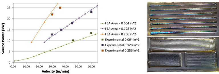
Experiments were performed with high power electron beam-based DED-AM, with processing powers ranging from 10 to 25 kW and velocities ranging from 30 to 60 ipm. The single bead parameters that were processed, along with a photograph of the processed substrate, are shown.
These results show strong agreement between the FEA simulation results and experiment.
The overarching objective of this project was to implement multi-sensor thermal imaging in commercially available DED-AM systems, and to couple this sensor data with process knowledge in order to develop tools to ensure a consistent and/or desired thermal profile.
Problem
Metal-based directed energy deposition additive manufacturing (DED-AM) and repair processes are in need of process monitoring and control technologies to improve process robustness. Recognizing that microstructure and distortion are driven by the thermal conditions during the build, end users need to have confidence that they can predict, control, and verify the thermal distribution in the deposit throughout the manufacturing process. Such technologies are critical for process certification and wider adoption within the aerospace and energy industries.
Objective
The overarching objective of this project was to implement multi-sensor thermal imaging in commercially available DED-AM systems, and to couple this sensor data with process knowledge in order to develop tools to ensure a consistent and/or desired thermal profile. Since the thermal history dictates microstructure development, achieving this objective promises to significantly reduce the need for costly and time-consuming post-process inspection.
An additional objective of this project was to ensure multi-sensor thermal imaging sensors were made available to end users through integration in commercially available AM systems.
Technical Approach
Technologies developed at PSU’s Center for Innovative Materials Processing through Direct Digital Deposition (CIMP- 3D) that enabled mapping of sensor data to X-Y-Z position during the deposition were integrated into commercial DED-AM systems. This involved transitioning both hardware modifications and custom software code to the AM Equipment Suppliers on the team.
Process map techniques originally developed at CMU were extended across a broader range of operating space. These process maps link power, velocity, and melt pool characteristics to prior grain structure during Ti-6Al-4V depositions. To capture results at both the low and high end of the energy spectrum, experiments were conducted on both the Optomec Laser Engineered Net Shaping (LENS) system at CIMP-3D and on Sciaky’s Electron Beam DM system. The results of this study were used to fashion and demonstrate a real-time microstructure controller.
Algorithms were developed to extract “thermal metrics” to reduce data from the thermal imaging sensors into a form that enabled correlation to microstructure variations occurring in three dimensions across the as-printed component. These reduced data sets were also compared to 3D computed tomography data from notional nozzle components, and showed evidence that such data can be used to identify flaws during processing.
Accomplishments
The developments in this project made significant strides in assessing the use of multi-sensor thermal imaging data for process monitoring and control of DED-AM processes.
Specific accomplishments include:
- Successful integration of Stratonic’s multi-sensor thermal imaging into a commercial Optomec LENS System.
- Expansion of CMUs Power-Velocity Process Maps (PV Maps) into the low and high power processing ranges. New relationships between melt pool geometry and prior grain structure were revealed in the low laser power regime, e.g. correlation between melt pool length, travel velocity, and microstructure. Critically, the melt pool length is observable and easily measured with a thermal image, thus enabling real-time control of solidification microstructure. These relationships were implemented into a real-time microstructure controller by CMU, Stratonics, and PSU on PSU CIMP-3D’s Optomec LENS system.
- Thermal metrics were developed and shown to correlate to various features of microstructure through collaboration between PSU and Wright State University (WSU). These were demonstrated using thermal data both from simulation and from multi-sensor thermal imaging, and results were published in peer-reviewed journals. Calibration of side-view thermal imaging was determined to require additional development, and a novel calibration method involving heating of a ceramic core with the DED-AM system laser was developed by PSU that shows promise. Additionally, PSU compared 3D visualizations of thermal metrics calculated from measured data against 3D computed tomography scans of completed parts, and demonstrated the potential to use thermal imaging to detect flaws.
Project Participants
Project Principal

Other Project Participants
- Stratonics
- Leonard Gelfand Center
- Sciaky
- ASM Education Foundation
- Optomec
- State College Area School District
- Carnegie Mellon University
- Wright State University
Public Participants
- U.S. Department of Defense
- National Science Foundation
- U.S. Department of Energy