

![]()
![]()
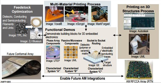
Interactions across the 3D printing value chain from feedstock optimization to equipment and software are all required to optimize the requirements of the multi-material printing process for 3D embedded electronics.
This project seeks to move from point solutions for complex electronic structures to a defined multi-material printed electronics solution that is modeled and characterized, providing the opportunity for an order of magnituge reduction in design-to-build cycle time and cost.
Problem
Current additive manufacturing (AM) technology has limitations in optimizing the production of integrated 3D printed electronics and nonplanar structures and components due to fragmented solutions in material, process, and design resulting in limited final product functionality and multi-material usage. Existing AM processes do not have the ability to construct integrated 3D electronics, conformal coatings, and structures during a single build. AM offers the opportunity to advance from 2D-constrained designs to conformal and embedded solutions that maximize functional capability while integrating electronic systems and minimizing footprint and impact on platform design.
Objective
The objective of this project was to advance multimaterial printing of integrated 3D electronics and nonplanar structures. The goal was to work across the supply chain to characterize and improve performance of an integrated system, instead of individual components, to realize robust multimaterial 3D and embedded fabrication processes. The intent was to demonstrate the characterized system and performance improvements by fabricating printed defense and commercial subsystems in a relevant production environment.
Technical Approach
This team’s approach was to apply its strength in printed electronics through an integrated system methodology to characterize commercially available inks. This included final properties and printability of inks (conductors and dielectrics) for low radio frequency (RF) to microwave frequency applications through improved process and process controls; control systems and deposition capabilities for multi-head printers; and design tools to support 3D multi-material configurations. Integrated systems of commercially available materials, printers, control software, and processes were detailed. Techniques were demonstrated by fabricating three subsystems using commercially available materials, equipment, and software, and by testing in a relevant production environment.
Accomplishments
The project focused on the defense demonstrator for advanced printing of microwave electronics led by Raytheon and the commercial demonstrator for an electrical structure used in a medical ultrasound application led by GE Global Research. The defense demonstrator was a C-band phased array single element with antenna designed by Raytheon and consisted of phase match tuner, quadrature couplers, band pass filter, antenna, and two monolithic microwave integrated circuit (MMIC) gallium arsenide low noise amplifiers (GaAs LNA). The defense demonstrator achieved excellent correlation between simulation and measured performance. Key features and accomplishments included fully printed multi-layer structures on couplers; fully printed circuits on all other passive elements; drilled and printed ground vias; active MMIC integration; AM printed interconnects from MMIC to circuit and between circuit elements; improved models and methods to characterize printable dielectrics; efficient characterization of inks up to 60 GHz; 3D printing of low dielectric constant (DK) materials; printability of Rogers low DK and low loss tangent material formulation developed within the project; and demonstration of a print/mill/print process for a fully printed coupler. The commercial demonstrator proved the feasibility to print a socket-to-socket interposer of dense high aspect ratio via field in 3mm thick low acoustic impedance materials operating at 5 MHz. The commercial demonstrator team delivered parts with electrical interconnects to the initial form factor that included high aspect ratio vias in polyetheretherketone (PEEK); drilling in multiple high temperature plastics at less than 200µms; and demonstration of a potentially higher yielding printed approach to the interposer with the vertical build and drill approach and the horizontal build with printed conductors.
Project Participants
Project Principal

Other Project Participants
- Univ. of Massachusetts-Lowell
- University of South Florida (USF)
- nScript
- Autodesk
- GE Global Research Center
- Rogers Corporation
Public Participants
- U.S. Department of Defense
- National Science Foundation
- U.S. Department of Energy